
Courtesy of Singapore-MIT Alliance for Research and Technology (SMART)
- This is the world’s smallest silicon (Si) light-emitting diode (LED) – smaller than the wavelength of light – with a light intensity comparable to much larger, state-of-the-art Si LEDs and with multiple potential applications
- This LED was used to build the world’s smallest holographic microscope and is a proof of concept that enables the cameras in existing devices (such as mobile phones) to be converted into high-resolution microscopes by only modifying the silicon chip and software
- Complementing this is a new neural networking algorithm developed by SMART that is able to reconstruct objects measured by this microscope, including plant seeds and tissue samples – allowing for enhanced microscopic examination of a wide range of objects that was not previously possible as well as the detection of plant disease and aberrant plant tissue
Singapore, 4 May 2023 – Researchers from the Disruptive & Sustainable Technologies for Agricultural Precision (DiSTAP) and the Critical Analytics for Manufacturing Personalized-Medicine (CAMP) Interdisciplinary Research Groups (IRG) of Singapore-MIT Alliance for Research and Technology (SMART), MIT’s research enterprise in Singapore have developed the world’s smallest LED (light emitting diode) that enables the conversion of existing mobile phone cameras into high-resolution microscopes. Smaller than the wavelength of light, the new LED was used to build the world’s smallest holographic microscope, paving the way for existing cameras in everyday devices such as mobile phones to be converted into microscopes via only modifications to the silicon chip and software. This technology also represents a significant step forward in the miniaturisation of diagnostics for indoor farmers and sustainable agriculture.
This breakthrough was supplemented by the researchers’ development of a revolutionary neural networking algorithm that is able to reconstruct objects measured by the holographic microscope, thus enabling enhanced examination of microscopic objects such as cells and bacteria without the need for bulky conventional microscopes or additional optics. The research also paves the way for a major advancement in photonics – the building of a powerful on-chip emitter that is smaller than a micrometre, which has long been a challenge in the field.

The light in most photonic chips originates from off-chip sources, which leads to low overall energy efficiency and fundamentally limits the scalability of these chips. To address this issue, researchers have developed on-chip emitters using various materials such as rare-earth-doped glass, Ge-on-Si, and heterogeneously integrated III–V materials. While emitters based on these materials have shown promising device performance, integrating their fabrication processes into standard complementary metal-oxide-semiconductor (CMOS) platforms remains challenging. While silicon (Si) has shown potential as a candidate material for nanoscale and individually controllable emitters, Si emitters suffer from low quantum efficiency because of the indirect bandgap, and this fundamental disadvantage combined with the limitations set by the available materials and fabrication tools has hindered the realisation of a small native Si emitter in CMOS.
In a recently published Nature Communications paper titled, “A sub-wavelength Si LED integrated in a CMOS platform”, SMART researchers described their development of the smallest reported Si emitter with a light intensity comparable to that of state-of-the-art Si emitters with much larger emission areas. In a related breakthrough, SMART researchers also unveiled their construction of a novel, untrained deep neural network architecture capable of reconstructing images from a holographic microscope in a paper titled, “Simultaneous spectral recovery and CMOS micro-LED holography with an untrained deep neural network” recently published in the journal Optica.
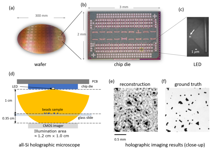
The novel LED developed by SMART researchers is a CMOS-integrated sub-wavelength scale LED at room temperature exhibiting high spatial intensity (102 ± 48 mW/cm2) and possessing the smallest emission area (0.09 ± 0.04 μm2) among all known Si emitters in scientific literature. In order to demonstrate a potential practical application, the researchers then integrated this LED into an in-line, centimetre-scale, all-silicon holographic microscope requiring no lens or pinhole, integral to a field known as lensless holography.
A commonly faced obstacle in lensless holography is computational reconstruction of the imaged object. Traditional reconstruction methods require detailed knowledge of the experimental setup for accurate reconstruction and are sensitive to difficult-to-control variables such as optical aberrations, the presence of noise, and the twin image problem.
The research team also developed a deep neural network architecture to improve the quality of image reconstruction. This novel, untrained deep neural network incorporates total variation regularisation for increased contrast and takes into account the wide spectral bandwidth of the source. Unlike traditional methods of computational reconstruction that require training data, this neural network eliminates the need for training by embedding a physics model within the algorithm. In addition to holographic image reconstruction, the neutral network also offers blind source spectrum recovery from a single diffracted intensity pattern, which marks a groundbreaking departure from all previous supervised learning techniques.
The untrained neural network demonstrated in this study allows researchers to use novel light sources without prior knowledge of the source spectrum or beam profile, such as the novel and smallest known Si LED described above, fabricated via a fully commercial, unmodified bulk CMOS microelectronics.
The researchers envision that this synergetic combination of CMOS micro-LEDs and the neural network can be used in other computational imaging applications, such as a compact microscope for live-cell tracking or spectroscopic imaging of biological tissues such as living plants. This work also demonstrates the feasibility of next-generation on-chip imaging systems. Already, in-line holography microscopes have been employed for a variety of applications, including particle tracking, environmental monitoring, biological sample imaging, and metrology. Further applications include arraying these LEDs in CMOS to generate programmable coherent illumination for more complex systems in the future.
Iksung Kang, lead author of the Optica paper and Research Assistant at MIT at the time of this research, said, “Our breakthrough represents a proof of concept that could be hugely impactful for numerous applications requiring the use of micro-LEDs. For instance, this LED could be combined into an array for higher levels of illumination needed for larger-scale applications. In addition, due to the low cost and scalability of microelectronics CMOS processes, this can be done without increasing the system’s complexity, cost, or form factor. This enables us to convert, with relative ease, a mobile phone camera into a holographic microscope of this type. Furthermore, control electronics and even the imager could be integrated into the same chip by exploiting the available electronics in the process, thus creating an ‘all-in-one’ micro-LED that could be transformative for the field.”
“On top of its immense potential in lensless holography, our new LED has a wide range of other possible applications. Because its wavelength is within the minimum absorption window of biological tissues, together with its high intensity and nanoscale emission area, our LED could be ideal for bio-imaging and bio-sensing applications, including near-field microscopy and implantable CMOS devices,” added Rajeev Ram, Principal Investigator at SMART CAMP and DiSTAP, Professor of Electrical Engineering at MIT and co-author of both papers. “Also, it is possible to integrate this LED with on-chip photodetectors, and it could then find further applications in on-chip communication, NIR proximity sensing, and on-wafer testing of photonics.”
This research was carried out by SMART and supported by the National Research Foundation (NRF) Singapore under its Campus for Research Excellence and Technological Enterprise (CREATE) programme.